![<?echo $_SERVER['SERVER_NAME'];?>](/template/twentyseventeen/skin/images/header.jpg)
The University of California, Berkeley, sponsored by semiconductor research firm SRC (Semiconductor Research Corporation), said recently that a three-dimensional packaging approach they are studying will dramatically improve the performance of smart mobile devices and wearable electronics. What's special about this research is that unlike the stacked chip package in the previous three-dimensional electronic interconnect solution, researchers tried to package a three-dimensional monolithic board with a semiconductor "ink" coating to add additional electronics. Transistor.
Through this latest electronic packaging process, semiconductor manufacturers will be able to develop smaller, more comprehensive, low-power, high-performance integrated components that dramatically increase the computing, storage, sensing, and display capabilities of their products. Due to the lower temperature generated by this processing technology, it is also suitable for high-polymer-based integrated circuits, providing more possibilities for applications in wearable electronic products and packaging materials.
According to Vivek Subramanian, a professor of electrical engineering and computer science at the school, "Our new approach is not only simpler to make, but also cost-effective than single-layer semiconductor crystal films, polysilicon gas storage or Other three-dimensional packaging technologies that are commonly used today. It may be even lower. We hope that through this research, the cost and performance ratio of the electronic components produced will be minimized."
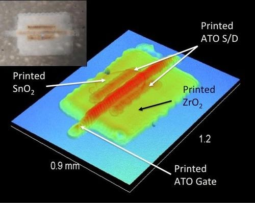
Currently, the team is investigating how to add additional active devices by spraying transparent oxide transistors directly on the surface of a CMOS (complementary metal oxide semiconductor) metal film.
To complement this research, materials and processing techniques also need to be modified to accommodate semiconductors, dielectrics, and conductors in the form of nanoparticles. The team is focusing on solution processing. Because the processing temperature is not high, compatibility with CMOS metal film is very good, and the production cost may be lower than other conventional methods.
According to Bob Havemann, director of the nanoprocessing science division at SRC, "Preliminary research by the Berkeley team shows that as long as the temperature of the process does not affect the metal film on the CMOS surface, the performance of the electronic integrated components packaged by the inkjet form can Was greatly improved."
Kleenex Ultra Soft,Kleenex Pocket Tissues,Kleenex Ultra Soft Tissues,Facial Paper
Baoda Paper Enterprise Co., Ltd. , https://www.baodatissue.com