![<?echo $_SERVER['SERVER_NAME'];?>](/template/twentyseventeen/skin/images/header.jpg)
Smart cards are ubiquitous in today's fast-paced economic life, and will gradually replace payment cards that store account information with magnetic strips. Smart cards are usually made into a pocket-sized card, similar to a standard credit card, in which an integrated circuit is embedded, typically a non-volatile memory or a secure processor with non-volatile memory. The smart card also has a plurality of electrical contacts embedded therein through which it can communicate with internal memory or the processor.
The core of the smart card lies in the processing and encryption functions of the embedded microcontroller, and the processing capability enhances the security. Due to the high cost of the smart card, the interface with the IC card needs to update the related infrastructure equipment, thereby slowing down the transition from the magnetic card to the smart card. However, as security requirements increase, especially as mobile phones and PDAs store more data, the demand for IC cards and other storage media (such as SD, miniSD, microSD, etc.) continues to increase. Both the Subscriber Identity Module (SIM card) and the payment terminal in the mobile phone can be regarded as smart cards.
In order to handle smart card transactions, a card reader that can securely access the embedded memory or processor is required to read the information and write the result back to the card. The physical size and signal interface of smart cards has been defined by standards organizations (such as ISO-7816), and organizations such as EuroCard, Mastercard, and Visa (EMV) have also established a set of standards for smart card addressing operations.
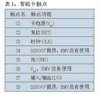
The electrical interface of the smart card consists of 8 contacts, arranged and embedded in the plastic card. See Table 1, 8 of the 8 contacts, only 5 EMVs, two of which are power and ground, and the other three are Signal contact, through which the card is read and written. C2 is the reset line, C3 is the clock line, and C7 is the serial I/O line.
Initially, the card specification specified a supply voltage of 5V ± 10% (Class A card), which has now been changed to 3V ± 10% (AB card), and later converted to 1.85V ± 10% (ABC class card). The ultimate goal is to phase out Class A cards in June 2009, leaving only Class AB or ABC cards.
Terminals that interface with smart cards must provide multiple supply voltages and appropriate signal levels. The interface specification also requires the terminal to withstand shorts between any two contacts of the card. Using a dedicated chip to provide the necessary power and signal levels is more advantageous than doing the same task with a large number of discrete devices. The DS8007 is a dedicated device that, in addition to the analog functions described above, includes FIFOs, processor interfaces, and timing control logic to support card communication.
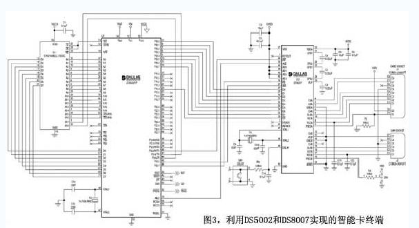
In order to better understand the work of the MCU and multi-protocol interface circuits, let us first study the basic steps of the smart card interface and communication with the card. We present an example of implementing a protocol and data transfer using the secure microcontroller DS5002 design interface terminal. The DS8007 interface circuit provides a signal interface, charge pump and voltage regulator to provide the appropriate power for the smart card. A dual smart card interface terminal can be formed by using two chips.
The RST and CLK signals are the inputs to the smart card and are provided by the interface terminals (DS5002 and DS8007). The reset signal is active low and the smart card can be reset asynchronously. In order to control the entire data transmission, a clock signal having a frequency ranging from 1 MHz to 5 MHz is connected to the clock contact (C3) of the smart card through a terminal interface. Finally, data is transferred from the smart card to the card reader via the I/O contact (C7) (send mode), or data is transferred from the card reader to the IC card (receive mode). The EMV specification states that the I/O contact of the smart card should be set to receive mode unless the I/O contact is transmitting data.
Terminal interface requirements
When the card is inserted into the terminal, the card contact is connected to the terminal contact and activated. The controller resets the card and then establishes communication between the card and the terminal through a series of characters (please refer to the acknowledge reset ATR); the next is the transaction processing. After the transaction is over, the contact is placed in the disabled state, after which the card can be pulled out or popped up. .
The ATR string establishes the initial communication information, including the specified protocol, bit timing, and subsequent data communication information. The ATR sequence includes an initialization character, a TS, and an additional 32 bytes of additional characters that are combined to inform the terminal how to communicate with the card in subsequent transactions. Subsequent data transfers can also change certain communication parameters, and ATR only establishes the most basic communication conditions.
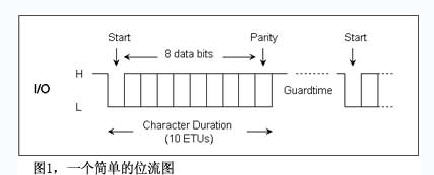
Each bit in the character transmission is defined as an elementary time unit (ETU), and the length of the ETU is linear with the CLK clock period of the smart card. The bit timing during ATR communication is called the initial ETU.
Any communication character contains 10 bits of data and lasts 10ETU. The first bit is the start bit, which is always low, and the I/O is high by default before the start bit. The last bit of each character is the check digit, which is determined by the sender. It may be high or low. The effect is to ensure that the number of 1s in the entire character is even. Figure 1 shows an example of a bit template, each character consisting of 10 bits, including 1 start bit, 8 data bits, and 1 check bit. Every two characters are separated by a minimum security period.
In the ISO-7816 specification, 4 bits are used to select the card communication protocol. Currently only two of the 16 protocols are used, named T=0 and T=1. Both of these are half-duplex modes (data can only be transmitted in one direction at any time) and asynchronous communication. T=0 is a character-based communication format, and T=1 is a data block-based communication format. All EMV-compliant smart cards must support the T=0 or T=1 protocol, and all terminals must support both protocols.
When the card is inserted into the terminal, all contacts remain low and the power supply VCC is immediately applied to contact C1. After confirming that the voltage is stable and meeting the specification limits, the terminal sets its own I/O contact to receive mode and provides a clock (CLK) signal to C3 of the card. In the 200 clock cycles from the start of the clock signal, the terminal must set the I/O port to a high-impedance state (receive mode), and the I/O port of the card is placed in the transmit mode.
After 40,000 to 45,000 clock cycles, the terminal sends a high level to the RST terminal of the card to activate the card. The card must send an ATR character answering terminal to the terminal within 400 to 40,000 clock cycles after the rising edge of RST. The ATR contains detailed information on subsequent communication operations, including the choice of T=0 or T=1 protocol. If no protocol is specified, the terminal default communication protocol is T=0.
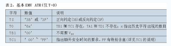
The first character of the ATR sequence is defined as the starting character TS. The first 4 bits of the TS contain 1 low start bit, then two high level bits, and finally a low level bit. This fixed bit template allows TS to synchronize information transmission. If the subsequent three bits of TS are all high-level, it means that the subsequent data is forward-principal decoding (when the data is transmitted, the low-order first); if these bits are all low, it means that the subsequent data is reverse-principal decoding. When the data is high, the high position is in the front). The EMV specification allows the use of reverse conventions, but it is recommended to use a positive convention in new card designs.
The last three bits of the TS consist of two low-level bits and one parity bit. The last bit of the 10-bit character frame is the parity bit. This bit level ensures that the number of 1s in this frame is even.
The second character of the ATR sequence is the format character, called T0. This character consists of two parts that are used to determine the characters contained in subsequent ATRs. The upper 4 bits of T0 are called Y1 and are used to indicate the subsequent transmission of TA1, TB1, TC1 or TD1. The transmission of 0~4 characters depends on how many positions 1 in Y1.
The lower 4 bits of T0 are denoted by K, representing the numbers 0 to 15, indicating the "history byte" contained in the subsequent ATR sequence. The "History Byte" provides general information about the card, such as the manufacturer of the card, the chip in the card, the ROM of the chip, or the expiration date of the card. Neither the ISO-7816 nor the EMV specification accurately defines this part of the information transmission.
If the ATR has a TB1 character, it passes the smart card's programming voltage requirements: b1 to b5 bits (called PI1) indicate the programming voltage; b6 and b7 (called II) indicate the maximum current required for programming. ATR compatible with basic EVM, TB1=00, indicating that VPP is not connected to the smart card.
The number N transmitted by the TC1 character determines the extra security time that needs to be added between two adjacent characters sent from the terminal to the smart card. This number does not affect the character transfer from card to terminal, nor does it affect the transmission of characters in two opposite directions. The binary number represented by N indicates the number of ETUs that are added for additional security time. When TC1 = FF, the shortest delay time is used between the two characters. In the T=0 protocol, this time is 12 ETUs. In the T=1 protocol, this time is 11 ETUs. N can be any number from 0 to 255. If the ATR does not contain TC1, the terminal will default to TC1=00 and continue with the subsequent work. Since N can add extra time during character transfer, it can minimize the input rate. Table 2 is a summary of the ATR for the T=0 protocol in the EMV specification.
Once the ATR process is over, the trading process begins. Regardless of the particular operation, the transaction is sent by the terminal to the smart card, and the smart card executes the instructions (and returns the execution result to the terminal). The operation of the card can be simply to specify a memory read operation, or it can be more complicated, such as performing an encryption operation. Either way, the communication between the terminal and the card is performed in accordance with the format of an Application Protocol Data Unit (APDU).
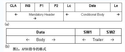
The special command information (C-APDU) sent by the terminal will generate a corresponding response message (R-APDU) from the card end, and this information is called an APDU command pair. The EMV specification defines these two instruction formats in detail. The basic structure of the instruction sent by the terminal must contain a 4Byte header, followed by a length-selectable data portion, as shown in Figure 2(a). The four bytes of the header include CLA, INS, P1, and P2, which specify the class of the instruction, the instruction code, and the parameters that support the particular instruction. The number of bytes of data following the C-APDU header is specified by the command Lc, and the number of bytes that the terminal expects the smart card response information to be specified by the instruction Le.
The response information (R-APDU) of the smart card is also composed of a plurality of bytes. As shown in FIG. 2(b), it is formatted into three segments, which are data (main body) and SW1, SW2 (tail) representing the command processing state. When the instruction is completed normally, the smart card returns the value of SW1 to 0x90 and the value of SW2 to 0x00. Other return values ​​indicate an operation error or a message is generated.
In order to handle all terminal transactions, the secure microcontroller DS5002 can be programmed to implement handshaking and data transfer protocols. We have developed some routines for the DS5002 and DS8007 (included in the DS8007 evaluation board) to implement the session between the terminal and the IC card, including power-on, ATR, APDU, and power down. If the EV kit is connected to a serial receive terminal, the EV kit and its software will transfer data over the RS232 serial port at a baud rate of 38400.
The detailed description of the software is beyond the scope of this article, but we can provide the source code of the basic smart card interface based on the DS5002 and interface chip DS8007 design scheme. The circuit of the design scheme is shown in Figure 3. The software is available from the an4029_sw.zip file in the directory. This file contains all the C code (main.c, ds8007.c, LCD Funct.c) and the assembly source code (Startup.a51) required to generate the HEX file (DS8007.hex). These code are compiled and linked using the Keil PK51 and mVision integrated development environment. The mVision project file (ds8007.Uv2) can also be found in this .zip file. After compiling, the .HEX file is downloaded to the DS8007 evaluation board and run.
To test the routines, we used a microcontroller-based smart card from ACS. This card can execute the embedded ACS smart card operating system version 1, or ACOS1. The card has the following features: 8kB E2PROM for storing application data, DES and MAC functions, process key based on random number, mutual authentication key pair, PIN code that cardholder can change, in accordance with ISO-7816-3 , T=0 agreement.
The ACOS1 file specifies that the IC card should return 19 bytes of reset data (ATR), and the value returned to T0 is 0xBE. The high nibble (0xB) indicates that TA1, TB1 and TD1 will appear in the ATR following the TS. The lower nibble (0xE) indicates that there are 14 history bytes in the ATR response. Therefore, the ATR transmitted from the card has a total of 19 bytes.
(Author: Frank Taylor, Maxim company)
Creative office
- Can be tailored at will, according to the needs of the site to tailor the appropriate size of office soft magnetic writing board, projectable and erasable dual-use soft magnetic writing board.,Whiteboard Wall.
- Support for custom corporate culture wall, production management record sheet, sales performance record sheet,etc.

Creative Office Products, Office Wallpaper,Office Whiteboard, Office Dry Erase Board
Guangzhou New Magnetics Technology Co.,Ltd , https://www.softwhiteboard.com